Sunday Thoughts: What happens when processors reach their physical limit?
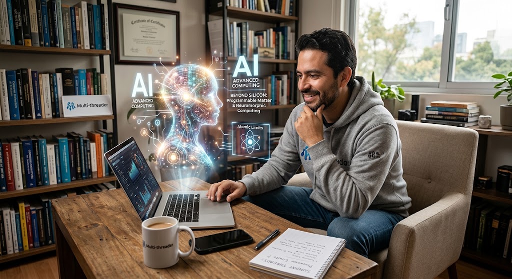
This Sunday, I found myself in a philosophical mood, pondering the fundamental physical limits of modern technology. For decades, the entire computing industry has comfortably relied on Moore's Law—continually shrinking transistors to make processors smaller, faster, and remarkably more efficient. However, we are rapidly approaching a hard boundary enforced by the fundamental laws of physics.
When transistor features reach the scale of just a few atoms, quantum tunneling causes electrons to leak through barriers, generating excessive heat and making predictable digital switching nearly impossible. So, what happens when processors simply cannot be made any smaller?
To explore this question, I spent part of my Sunday having a fascinating conversation with AI, brainstorming potential paradigms that could reshape computing once traditional silicon scaling hits a wall.
The Sunset of Traditional Silicon Scaling
For years, computer architecture relied on Dennard scaling and photolithography advances to push transistor counts higher. But as we reach sub-nanometer scales, physical constraints dominate:
- Quantum Tunneling: At atomic scales, electrons jump across insulating barriers, creating current leaks and computational errors.
- Thermal Dissipation Limits: Power density becomes so high that cooling ultra-dense silicon blocks without damaging the chip becomes prohibitively difficult.
- Economic Limits: Building semiconductor fabrication plants (fabs) for advanced nodes now costs tens of billions of dollars, creating an economic bottleneck alongside the physical one.
If we can no longer rely on physical miniaturization, the industry must innovate at the structural, architectural, and material levels.
Beyond Silicon: Emerging Computing Technologies
During my discussion with AI, we explored several emerging alternatives that move beyond simply squeezing more transistors onto a flat piece of silicon.
1. Programmable Matter (Claytronics & Reconfigurable Materials)
One of the most mind-bending concepts we discussed was programmable matter—materials engineered to dynamically alter their physical properties (shape, density, optical attributes, or electrical conductivity) on command via embedded software or external control fields.
In computing, instead of manufacturing rigid, static microchips, programmable matter could allow hardware to physically reconfigure its topology in real time depending on the algorithm being executed. Imagine a chip whose physical circuits morph into an optimal layout for neural network training one second, and restructure themselves for cryptographic hashing the next.
2. Neuromorphic Computing
Rather than adhering strictly to the traditional Von Neumann architecture—where processor and memory are separated by a bus that creates performance bottlenecks—neuromorphic computing takes direct inspiration from biological brains.
Using specialized hardware components like memristors, neuromorphic chips integrate memory and computation directly into artificial neurons and synapses. They operate on asynchronous event-driven pulses (spikes), consuming orders of magnitude less power while excelling at pattern recognition, sensory processing, and real-time AI workloads.
3. Photonic & Optical Computing
Electrons traveling through copper traces generate resistance and heat, inherently limiting clock speeds. Photonic computing replaces electrons with photons (light particles) to perform calculations and transmit data.
By utilizing optical waveguides, beamsplitters, and lasers, photonic processors can calculate complex matrix operations at the speed of light with virtually no thermal loss. While full general-purpose optical CPUs remain challenging, hybrid optical-electronic accelerators are already demonstrating immense promise for AI inference and high-throughput vector math.
4. 3D Monolithic Stacking & Chiplets
If we cannot shrink components horizontally, we must build vertically. 3D Monolithic Integration stacks logic, memory, and interconnect layers directly on top of one another using ultra-dense Through-Silicon Vias (TSVs) or direct molecular bonding. Combined with modular chiplet architectures, this allows heterogenous integration—coupling different optimized silicon technologies (such as high-bandwidth memory, optical transceivers, and specialized AI accelerators) into a single cohesive package.
Final Thoughts
Reaching the physical limit of traditional silicon isn't the end of computing progress; it is simply the catalyst for a paradigm shift. We are moving away from brute-force miniaturization toward architectural creativity, bio-inspired designs, and fundamentally new physical mediums like light and programmable matter.
What are your thoughts on where computing is headed? Do you think programmable matter or optical chips will be the true successors to silicon? Let me know in the comments below!